
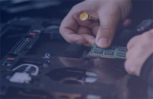
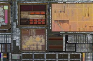
ARE YOU LOOKING FOR A CAREER IN VLSI & EMBEDDED SYSTEMS?
Classroom | Online | Hybrid | eLearning Courses
100% job oriented VLSI training courses

Are you a Working professional Upgrade your skill
VLSI Guru Training Institute
100% job oriented VLSI training courses
Offline, Online and Hybrid model
(Offline & Online) Training Available.
VLSI Guru Training Institute

Looking for Internship
VLSI Guru Training Institute
100% job oriented VLSI training courses
Upgrade Your Skill Set
VLSI Guru Training Institute
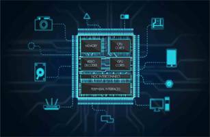
Institute offers 30+ unique courses in VLSI domain


Dhanush T
Very good Institute for the VLSI courses. They are always ready to provide the help required. The courses are very well designed, and lab sessions gives you hands on experience. Once you complete the course, you will be very well equipped to clear interview and land in good job.
3 Month Ago

Kolli Aravind Chinnu
I have taken DFT course online. Institute is student friendly, and is professional at the same time. Classes are nicely taken from the experienced. Labs are great and we will learn a lot. The inputs from faculty are nice.
3 Month Ago

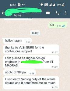
Digital Design Enginner In analog device
7 Days Ago
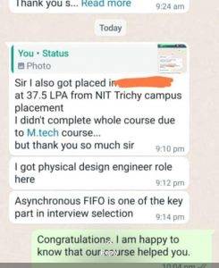
Physical Design Engineer
7 Days Ago