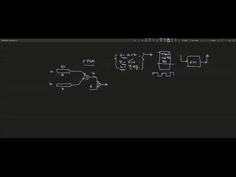
FPGA System Design training is a 6 months course provides participants with wider and deep understanding of the FPGA Architecture, Design, Timing closure flow and debugging.
Next Batch
1-1 Dedicated Mentor Support
24/7 Tool Access
Multiple Mock Interviews
Industry Standard Projects
Support with Resume Update
FPGA System Design Training Overview
The FPGA System Design Course is an advanced 8-month industry-oriented training program that provides participants with comprehensive, hands-on expertise in FPGA architecture, RTL-based FPGA design, timing closure, FPGA implementation, FPGA debugging, and FPGA prototyping and validation workflows.
This FPGA training program is designed for both RTL design engineers and verification engineers who want to gain deep practical exposure to the complete FPGA system design flow — from architecture understanding and RTL coding to timing closure, IP integration, embedded system bring-up, and hardware debugging on real FPGA boards.
Why This FPGA System Design Course?
Modern semiconductor and product companies rely heavily on FPGA-based prototyping and validation to accelerate chip development cycles. Engineers who can confidently handle FPGA design, timing closure, and FPGA debugging are in high demand across ASIC prototyping, embedded systems, and hardware verification teams.
This course is built to develop exactly those skills — combining insightful lectures with structured lab sessions and multiple hands-on FPGA projects that give participants real-world exposure to the complete FPGA development flow.
What You Will Learn
- FPGA Architecture — deep understanding of internal FPGA architecture, resources, and fabric organization
- FPGA Internals & I/O — CLBs, DSP blocks, BRAMs, PLLs, I/O standards, and high-speed interface management
- RTL-Based FPGA Design — implementing FPGA designs using Verilog HDL and VHDL following industry coding practices
- IP-Mode FPGA Implementation — integrating pre-built IP cores for rapid FPGA system development
- FPGA Timing Closure — mastering timing constraints, setup and hold analysis, clock domain crossing, and timing violation resolution using Vivado
- Vivado Design Flow — complete Xilinx Vivado tool flow including synthesis, implementation, and bitstream generation
- FPGA Debugging — hardware debugging using Vivado ILA, waveform analysis, chipscope debug, and signal probing techniques
- Software Development Kit (SDK/Vitis) — embedded software development for FPGA-based systems
- FPGA Booting & Embedded Linux — booting FPGA platforms with PetaLinux and Ubuntu for embedded system applications
- FPGA Prototyping & Validation — using FPGAs as prototyping platforms for ASIC and SoC design validation
Hands-On, Project-Driven Training
Every session in this FPGA System Design course is planned with practical coding examples, lab exercises on real FPGA boards, and hands-on projects covering the complete FPGA system design flow. Lab sessions are scheduled at regular intervals to reinforce concepts immediately after theory modules — ensuring participants develop genuine confidence working with FPGA hardware and EDA tools.
The course places special emphasis on plug-and-play FPGA board experience, so participants leave with the ability to independently set up, program, debug, and validate designs on real FPGA hardware.
Who Should Enroll
This FPGA System Design training is the right choice for:
- RTL design engineers looking to gain expertise in FPGA implementation and timing closure
- Verification engineers planning to move into FPGA prototyping and hardware validation roles
- Fresh graduates targeting careers in FPGA design, embedded systems, or ASIC prototyping
- Experienced engineers from other domains planning to transition into FPGA-based system design and development
- Engineers targeting roles in FPGA-based product companies, ASIC prototyping teams, and embedded hardware teams
Questasim, Vivado, Zed board


Key Features

Who All Can Attend This FPGA System Design Training?
This training is ideal for professionals aiming to gain practical knowledge in designing, implementing, and debugging digital systems using FPGAs. It is suitable for both entry-level and experienced engineers working in embedded systems, hardware design, or VLSI domains.Pre-requisites To Take FPGA System Design & Verification
- Expertise to C programming
- Exposure to Digital design basics

High Demand for FPGA System Design & Verification
Know about the Growing VLSI industry
FPGA Design Engineers are in high demand in industries like telecom, aerospace, and automotive. Salaries increase with experience in RTL design, IP integration, and proficiency in tools like Vivado or Quartus. Bangalore and Hyderabad offer the highest compensation due to strong semiconductor ecosystems.
₹12 LPA
₹15 LPA
₹18 LPA
₹20 LPA


FPGA technology plays a critical role in modern electronics, powering applications in communication, automotive, AI hardware, and embedded systems. A structured FPGA System Design training program helps candidates develop the ability to design, simulate, and implement digital systems on real hardware platforms.
\n\n
For beginners, enrolling in an FPGA System Design course for freshers or an FPGA System Design training for freshers provides a strong foundation in RTL design, synthesis, and FPGA prototyping. A well-designed FPGA Design training approach ensures that learners understand both theoretical concepts and real-time hardware implementation.
\n\n
Learn Through Real-Time Projects and Practical Implementation
\n\n
The effectiveness of an FPGA System Design training course depends on hands-on exposure. Programs offering FPGA System Design training with real projects enable learners to work on real-time applications, improving their understanding of timing analysis, hardware debugging, and system integration.
\n\n
An advanced full FPGA System Design training includes Industry Standard Projects, structured assignments, and implementation on FPGA boards. With real time FPGA System Design training with internship, candidates gain practical exposure to real industry workflows.
\n\n
Learners can opt for flexible FPGA Online Training or choose an offline FPGA System Design training institute for classroom-based learning, depending on their preference.
\n\n
Internship Programs That Enhance Job Readiness
\n\n
Practical experience is essential for building a successful FPGA career. A well-structured FPGA System Design training and internship or an FPGA System Design internship program with placement provides real-time exposure to industry practices.
\n\n
Programs offering an FPGA System Design internship with placement support or an FPGA System Design internship for freshers help candidates gain confidence and hands-on expertise. A comprehensive FPGA System Design course with internship and placement ensures that learners are prepared for real-world challenges.
\n\n
These programs are ideal for those seeking a job oriented FPGA System Design course with strong practical exposure.
\n\n
Designed for ECE, EEE, and Engineering Graduates
\n\n
A focused FPGA System Design training for ECE students and FPGA System Design training for EEE students helps candidates from core electronics backgrounds transition into FPGA and embedded roles.
\n\n
Programs designed as FPGA System Design training for fresh graduates with placement ensure that learners gain both conceptual clarity and hands-on skills. A comprehensive FPGA System Design training program prepares candidates to handle real-time system design challenges effectively.
\n\n
Placement-Focused Training for Career Growth
\n\n
A placement oriented FPGA System Design course plays a crucial role in helping candidates secure jobs in FPGA and embedded domains. Programs offering FPGA System Design training with placement include resume building, technical preparation, and Mock Interviews.
\n\n
A FPGA System Design course with placement assistance ensures that candidates are fully prepared for recruitment processes. Enrolling in an FPGA System Design course with job assistance or an FPGA System Design course with job assurance aligns your skills with current industry expectations.
\n\n
For faster career entry, fast track FPGA System Design training options provide accelerated learning while maintaining strong practical exposure.
\n\n
Learn with Expert Guidance and Flexible Options
\n\n
A high-quality FPGA Training Institute provides structured learning supported by experienced mentors. With Expert Faculty Support, learners receive continuous guidance throughout the course.
\n\n
Flexible options like a weekend FPGA System Design training course make it easier for students and working professionals to upskill. Regular doubt clarification sessions ensure that learners can resolve challenges quickly and stay consistent in their progress.
\n\n
Start Your Career in FPGA System Design
\n\n
With increasing demand for FPGA engineers across industries, enrolling in an FPGA System Design training near me or a comprehensive training program is a smart career move. Choosing the best FPGA System Design training institute ensures access to quality learning, internships, and placement support.
\n\n
A complete job oriented FPGA System Design training equips you with both technical expertise and real-time experience. With the right combination of training, internship, and placement assistance, you can confidently step into FPGA and embedded system design roles and build a successful career.

Explore a wide range of VLSI and Embedded Systems courses to get industry-ready.
50+ industry oriented courses offered.

Explore a wide range of VLSI and Embedded Systems courses to get industry-ready.
50+ industry oriented courses offered.