Custom and analog layout basics (3 months)
- Requirements
- Design specification & architecture
- RTL Coding
- RTL integration
- Functional verification
- Synthesis
- DFT
- Physical Design
- STA
- Custom Layout
- Physical Verification
- Post Silicon Validation
- Combinational logic
- Number systems
- Radix conversions
- K-maps, min-terms, max terms
- Logic gates
- Realization of logic gates using mux’s and universal gates
- Compliments (1/2/9/10’s complement)
- Arithmetic operations using compliments
- Boolean expression minimization, Dmorgan theorems
- POS and SOP
- Conversion and realization
- Adders
- Half adder
- Full adder
- Subtractor
- Half subtractor
- Full subtractor
- Multiplexers
- Realizing bigger Mux’s using smaller Mux’s
- Implementing Adders and subtractors using Multiplexers
- Decoders and Encoders
- Implementing Decoders and Encoders using Mux and Demux
- Bigger Decoder/Encoder using smaller Decoder/Encoder
- Comparators
- Implementing multi bit Comparators using 1-bit Comparator
- Sequential logic
- Latch, Flipflop
- Latch, Flipflop using Gates or Mux’s
- Different types of FFs
- FF Truth table
- Excitation tables
- Realization of FF’s using other FF’s
- Applications of FF’s, Latches
- Counters
- Shift registers
- Synchronizers for clock domain crossing
- FSM’s
- Mealy, Moore FSM
- Different encoding styles
- Frequency dividers
- Frequency multiplication
- STA
- Setup time, Hold time, timing closure
- fixing setup time and hold time violations
- Launch flop, capture flop
- Unix Operating System
- Kernel
- Unix Shells, RC files
- Shell scripting basics (as required for job)
- Unix Directory structure, hard/soft links
- Xterm, Xhost, commonly used commands
- Text editors
- Revision Management
- Makefile, Cronjob
- Mapping Unix directories, file with Gvim editor
- FTP, SCP, Mail, Compress, sleep, regular expressions
- LSF, Batch submission, Process monitoring
- Revision Management with hands on labs
- Basic Passive and Active devices.
- Ohms law, Kirchoff laws
- Basic of circuit understanding
- Transistors in hardware design
- Significance of transistors in hardware design
- Logic gate implementation using BJT, CMOS
- MOSFET functionality
- Semiconductors
- What makes Semiconductor special element?
- Classification of solids into three types
- Conductor, Insulator, Semiconductor
- Energy bands in Solids
- Types of Semiconductors
- Intrinsic Semiconductors
- Extrinsic Semiconductors
- Types of Extrinsic Semiconductors
- N-type Extrinsic Semiconductor
- P-type Extrinsic Semiconductor
- Si, Ge – comparison
- Types of current in Semiconductors – Drift, Diffusion
- ion
- PN Junction dioda
- PN Junction – forward, reverse bias
- V-I Characteristics of PN Junction Diode
- Different types of Diode
- Applications of Diode
- BJT
- BJT
- BJT working principle?
- How BJT can be used for large scale manufacturing
- BJT fabrication steps
- Types of BJT?
- Why BJT is not used in for lower technology nodes?
- Issues with BJT?
- Advantages of BJT?
- NAND gate using BJT?
- Field Effect Transistor : FET
- What is Field Effect Transistor?
- Types of FET
- NMOS
- PMOS
- CMOS
- Fin
- NMOS
- NMOS
- What is NMOS?
- NMOS working principle?
- Different voltages, currents, their equations
- NMOS circuit representation
- How NMOS works like a switch
- How NMOS can be used for large scale manufacturing
- NMOS fabrication steps
- Types of NMOS?
- Why CMOS is used instead of NMOS?
- Issues with NMOS?
- Advantages of NMOS?
- NAND gate using NMOS?
- CMOS
- CMOS
- What is CMOS?
- CMOS working principle?
- Different voltages, currents, their equations
- CMOS circuit representation
- How CMOS works like a switch
- How CMOS can be used for large scale manufacturing
- CMOS fabrication steps
- Types of CMOS?
- Issues with CMOS?
- Advantages of CMOS?
- NAND gate using CMOS?
- CMOS second order effects?
- FinFET
- FinFET
- What is FinFET?
- FinFET working principle?
- Different voltages, currents, their equations
- CMOS circuit representation
- How CMOS works like a switch
- How FinFET can be used for large scale manufacturing
- FinFET fabrication steps
- Types of FinFET?
- Issues with FinFET?
- Advantages of FinFET?
- NAND gate using FinFET?
- Layers of CMOS
- Depositing oxide layer
- Photholithography
- Masking
- Ethching Layers
- Formation of nwell
- Self aligned gate fabrication process
- Diffusion to create n+ and P+ regions
- Metallization
- Overview
- Env Setup
- Special Variables
- Data Types
- Variables
- Operators
- Decisions
- Loops
- Arrays, Strings, Lists, Dictionary
- History and Redoing of commands
- String Pattern Matching commands
Custom and analog layout advanced (5 months)
| Synopsys Tools | Cadence Tools |
|---|---|
|
|
- Layout Editor Tool
- Understanding the schematic symbols and parameters
- Creating and managing libraries and cell
- Commands for Layout editing.
- Commands for schematic editing.
- Verification : DRC and LVS
- Antenna effect, latchup, Electromigration, IR Drop
- Analog Layout of OpAmp, Current Mirror, PLL, ADC, and DAC
- Resistor, Capacitor layout techniques
- CMOS and BiCMOS layout techniques
- Standard Cell Layout : Inverter, AND, OR, NAND, NOR, AOI, OAI, Latches, and Flop
- Schematic entry
- Early parasitics
- Estimated parasitic assistant
- Reliability analysis
- Static circuit checks(CCK)
- Early parasitics
- Pre-layout simulation and analysis
- Standard cells
- Analog circuits
- Analog and mixed mode circuits
- Layout
- Analog and Digital co-design
- Fusion compiler co-design
- IC Compiler II co-design
- IC Compiler co-design
- In-design error checks
- DRD
- IC Validator live DRC
- Via checks
- Metal Density analysis
- Color decomposition
- In-design electrical checks
- Electro migration
- Resistance
- Capacitance
- Shield coverage
- Voltage annotation for VDRC
- Early parasitics
- Estimated parasitic assistance
- Partial layout extraction
- Power device design
- Power device designing
- Analog design migration
- Schematic migration
- Layout migration
- Analog and Digital co-design
- Mismatches and Matching
- Techniques
- Inter digitization
- Common centroid
- Techniques
- Failure Mechanism
- Electro migration
- IR drop
- LOD & Stress effects
- WPE, Antenna Effects
- Latch up
- ESD
- High voltage rules
- EOS effects
- Noises & Coupling
- Different Types of process
- Advantages & Disadvantages of below
- Planar CMOS
- FD-SOI
- SOI
- Bi-CMOS
- Gallium Arsenide
- Silicon-Germanium
- Finfet
- Full Chip Construction
- Scribe Seal
- Pad Frame
- Integration and guidelines
- Packaging
- Std Cell & Memories.
- IO Layout Guidelines : High speed IOs and High Speed Interfaces.
- Sense amplifier & Bit cell development
- Why memory layout different than analog layout
- Memory layout flow
- Types of memory layout (SRAM/DRAM/ROM)
- Introduction to SRAM memory layout
- Fixing few manually created leaf-cell errors which impact
- Abutment issues
- Impact of IR, EM and DFM .
- SRAM memory design architecture
- Words line and address line
- SRAM rows and column design
- Building blocks of SRAM
- Memory Bit cell
- Row decoder
- Word line driver
- Sense amplifier
- Control block
- Misc digital logic.
- Pitch Calculation for blocks.
- Power Planning
- High speed Analog Layout
- RF Layout guidelines with Transmission lines and inductor concepts
- Handling clocks
- Analog Circuits & Layout guidelines
- Single & Multi stage differential opamp layout
- current mirror layout
- PLL, DLL and Oscillators
- LDO and other regulators
- ADCs & DACs
- Bandgap, Temperature sensors & Biases -> Current & Voltage bias lines
- Large drivers
- input pair, differential routing, Power routing, offset minimising
- Power/Signal IR Drop
- cross-talk and coupling
- Electrostatic Discharge
- Deep Sub-micron Layout Issues
- Shallow Trench Isolation (LOD)
- Well Proximity Effect
- Design Rule Checks
- Layout Versus Schematic (LVS)
- Electrical Rule Checks (ERC)
- Antenna Checks
- Latch-up
- Reliability checks like EM and IR analysis
- Design for manufacturability (DFM)checks
- Electrostatic discharge (ESD) path checks
- Assignments and multiple hands on projects
- Best Practices & Interview Questions.
Course Overview
Tools:Synopsys Custom designer and Cadence Virtuoso tools (24×7 Tool access)
- Analog Layout, Memory Layout, Standard Cell and IO Layout Design
- CMOS, FinFET technologies and various memory architectures
- Detailed understanding of VLSI Design Flow and Advanced Digital Design
- Linux commands, scripting, version control, and soft skills for interviews
- Semiconductors, Ohm’s Law, Kirchhoff’s Laws
- Diode and MOSFET operation with second-order effects
- FinFET technology and complete IC fabrication process
- Standard Cell Layout Design
- Memory Layout and IO Layout for multiple architectures
- Analog Layout Techniques including Matching and Noise Mitigation
- Analysis of Electro Migration, IR Drop, Antenna Effect, WPE, LOD, Latch-up, and ESD issues
- 20+ lab sessions and detailed assignments across all layout areas
- Real-time projects in Standard Cell, IO, Memory, and Analog Layout
- Common Centroid and Interdigitation Techniques
- Resistor and Capacitor Matching
- Opamp Layout, Current Mirrors, PLLs, ADCs, DACs
- Bandgap References, Temperature Sensors
- Current and Voltage Bias Lines, Large Drivers, LNAs, Mixers
- Sense Amplifier and Bit Cell Development
- Comprehensive theory + lab sessions guided by industry experts
- Practical exposure using real-time design examples
- End-to-end Custom Layout expertise from basics to advanced analog design
- Emphasis on failure mechanisms and robust layout strategies
- Industry-standard practices and tools throughout the course
- Institute Info:
- Offered by VLSIGuru, established in 2012
- Trained over 10,000+ students
- Affordable in-class training in Bangalore
- Online training available for students outside Bangalore
Detailed overview:
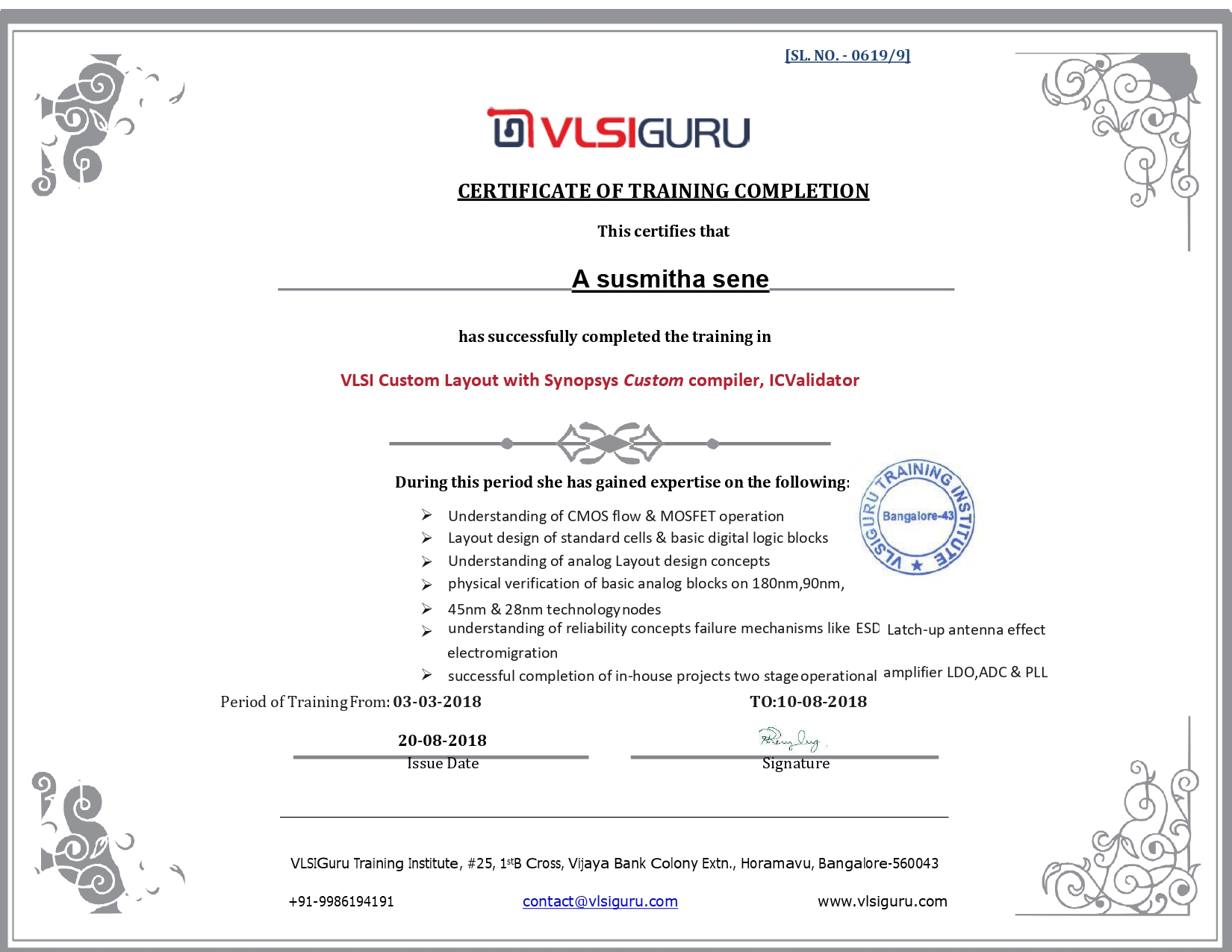
Custom layout training is a 8 months course focused on all the aspects of layout including Analog layout, Memory layout, Standard cell layout and IO layout.
Custom layout design course ensures that the student is prepared on all the essential aspects of Custom layout including VLSI Design flow, advanced digital design, CMOS, FinFET, various memory architectures, Standard cell, IO’s and detailed analog layout techniques. Course also includes training on Linux commands, version control, scripting and soft skill for effective interview performance.
Course also includes detailed sessions on semiconductors, Ohms law, Kirchoff law’s, Diode-operation, MOSFET’s, MOSEFT operations, second order effects, FinFET’s, and detailed fabrication process, which is followed by assignments and hands on projects.
Course also covers layout basics, hands on standard cell layouts, IO layout and memory layout for different architectures. Followed by various analog layout techniques with detailed discussion on Mismatches & Matching, Noises & Coupling, various failure mechanisms which includes Electro migration, IR drop, LOD & Stress effects, WPE, Antenna Effects, Latch up, ESD. Course includes 20+ detailed labs & assignments covering all aspects of custom layout with multiple hands on projects.
Analog layout techniques involve multiple hands on projects covering various concepts such as common centroid, inter digitation, resistor matching, capacitor matching and opamp circuits, current mirrors, PLL’s, ADC’s, DAC’s, Bandgap, Temperature sensors & Biases -> Current & Voltage bias lines, Large drivers, LNA & Mixers, and Sense amplifier & Bit cell development.
Projects are the most significant part of any engineers(both fresher and experienced) resume. It is the projects that differentiate your resume from other resumes, which essentially helps your chances of getting through the interviews.
Below is the list of projects student will be doing as part of eight months training. Student will be doing all these projects from scratch. These projects will provide student with expertise on par with a 2 to 3 years experienced engineer, in terms of all the skill set required. Student can work on additional projects to enhance resume for experienced job role.
By working on below projects, student will get familiar with:
- Complete layout flow including
- Floor planning
- Schematic
- Layout
- Physical verification
Description : Schematic, Layout design and verification for standard cell for NOT, NAND, NOR, AND, OR gate and Buffer.
Role : Layout Design and Layout Verification.
Challenges : Involved in placement, routing by taking care of minimum area and Verification.
Tools Used : Synopsys Custom Designer & IC Validator (for DRC/LVS).
Technology Node: 28nm
Description : Designed the layout for 4 bit Digital to Analog converter. Main Challenge was the matching of the resistors.
Role : Layout Design for block level. Adjusted M1 and M2 pattern errors by adding fill cells and metal fills cleaned DRC, LVS by using the CPDS.
Challenges : Floor-planning considering resistor. Routing is one by taking care of IR, symmetry and top-level layout verification.
Tools Used : Synopsys Custom Designer & IC Validator (for DRC/LVS).
Technology Node : 28nm
| Course | Custom and analog layout training |
|---|---|
| Duration | 8 months |
| Next Batch | 27/July |
| Schedule | |
| Freshers | 6 days/week, 9:30AM to 1:30PM Access to all session videos for 10 days for every session |
| Working professionals | Saturday, Sunday, 9:30AM to 6:30PM 9:30 to 1:30PM : Theory 2:30PM to 6:30PM : Labs Access to all the course recorded videos |
| New batch starts | Every 5 Weeks |
| Tools | SYNOPSYS,CADENCE {Synopsys Custom Designer, IC Validator} |
| Mode of training | Live(offline and online) training eLearning also available |
| Tool Access | Tool access for complete course duration |
| Batch Size | 15 |
demo video using Synopsys Custom Compiler
demo video using CADENCE VIRTUOSO
- Expertise on Digital & Analog design concepts
- Exposure to basic layout concepts
- Course presentations for all topics
- Session notes
- Lab documents with detailed steps
- User guides
Experienced Trainer
- 6+ years of rich experience of working in all aspects of custom layout from Analog, Memory, IO and Standard cell at various technology nodes
- Senior Director in a reputed Design company