DDR is an essential component of every complex SOC. It requires every engineer working on SoC to be well versed with DDR protocol concepts including DDR controller, DDR PHY, DDR memory, etc.
Next Batch
1-1 Dedicated Mentor Support
24/7 Tool Access
Multiple Mock Interviews
Industry Standard Projects
Support with Resume Update
DDR5 Training Overview
Course Overview
DDR5 protocol training is focused on understanding of all the aspects of DDR5 including DDR5 ports, commands, timing diagrams, training sequences, post package repair, ODT etc.
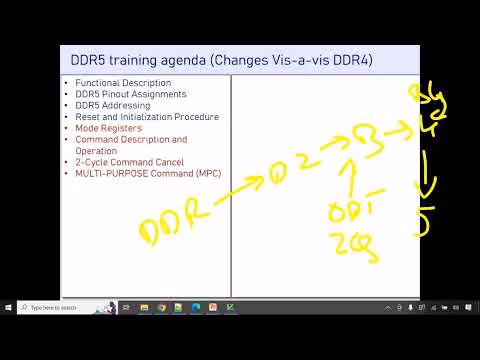
Functional Description
DDR5 Pinout Assignments
DDR5 Addressing
Reset and Initialization Procedure
Mode Registers
Command Description and Operation
2-Cycle Command Cancel
MULTI-PURPOSE Command (MPC)
2N Mode
CS Geardown Mode
ACTIVATE Command
PRECHARGE Command
IO Features and Modes
Programmable Preamble and Postamble
Interamble
On-Die ECC
Write Operations
READ Operations
Temperature Sensor
REFRESH Operation
Self Refresh Operation
Input Clock Frequency Change
Power-Down Mode
Maximum Power Saving Mode
Connectivity Test Mode
ZQ Calibration Commands
Per-DRAM Addressability
CS Training Mode
CA Training Mode
Write Leveling (WL) Training Mode
Read Training Pattern
Read Preamble Training Mode
Post Package Repair
Memory BIST Post Package Repair (mPPR)
On-Die Termination

Key Features
Who All Can Attend This DDR5 Training?
This DDR5 Training is designed for professionals looking to specialize in next-generation memory technologies, focusing on DDR5 architecture, interface design, and validation techniques. It's ideal for engineers involved in high-speed memory systems and SoC integration.Pre-requisites To Take DDR5 Training
- Exposure to basic memory concepts like SRAM, FLash, etc
- Exposure to digital design concepts
High Demand for DDR5 Training
Know about the Growing VLSI industry
Protocol Design Engineers are responsible for defining and implementing USB4 protocol stacks and ensuring compliance with USB4 specifications.
With USB4 adoption rapidly growing across consumer and enterprise devices, there’s an increasing demand for engineers who can design robust, high-speed serial protocols.
Companies like Intel, AMD, Qualcomm, and Synopsys actively hire for this profile.
₹6 LPA
₹10 LPA
₹16 LPA
₹22 LPA
₹30+ LPA


Explore a wide range of VLSI and Embedded Systems courses to get industry-ready.
50+ industry oriented courses offered.

Explore a wide range of VLSI and Embedded Systems courses to get industry-ready.
50+ industry oriented courses offered.